
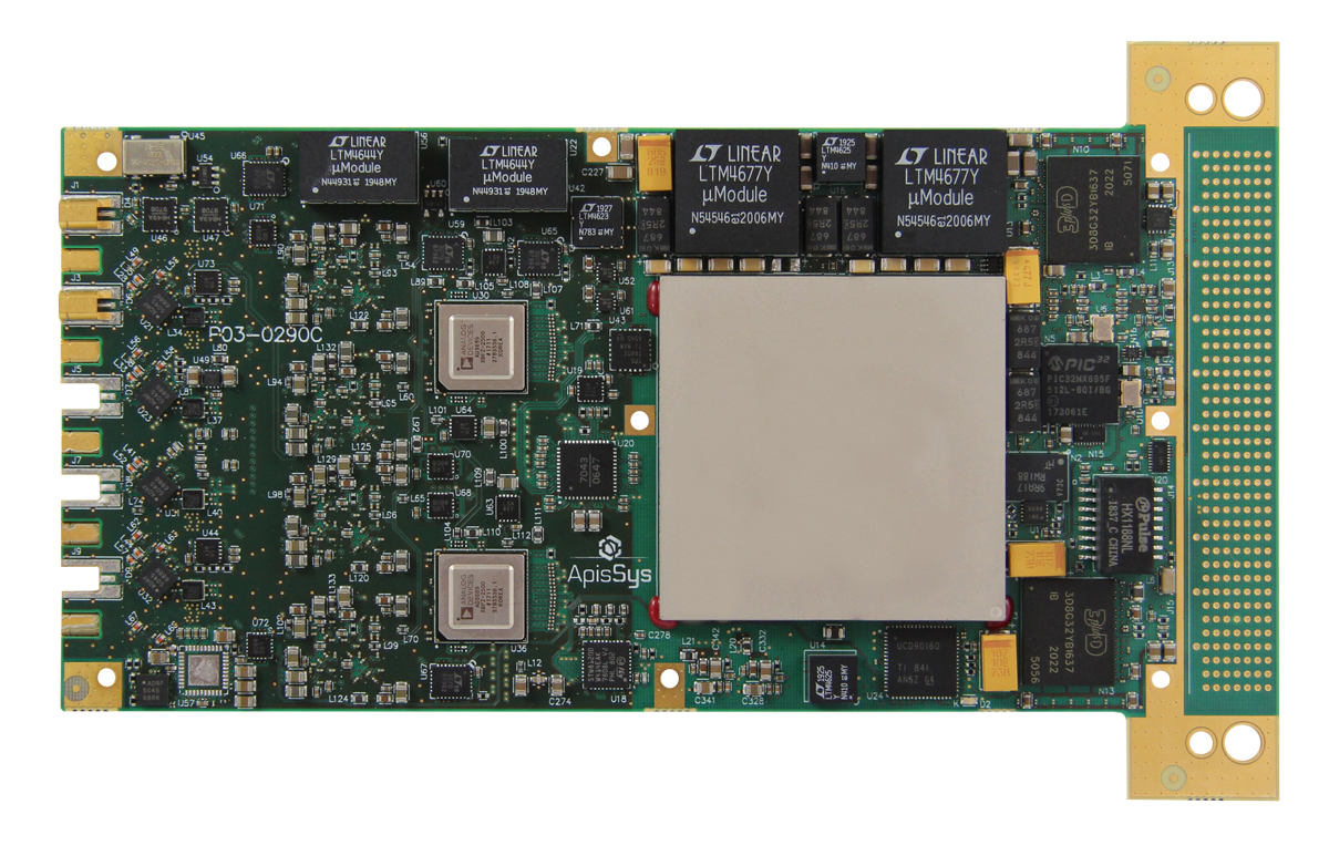
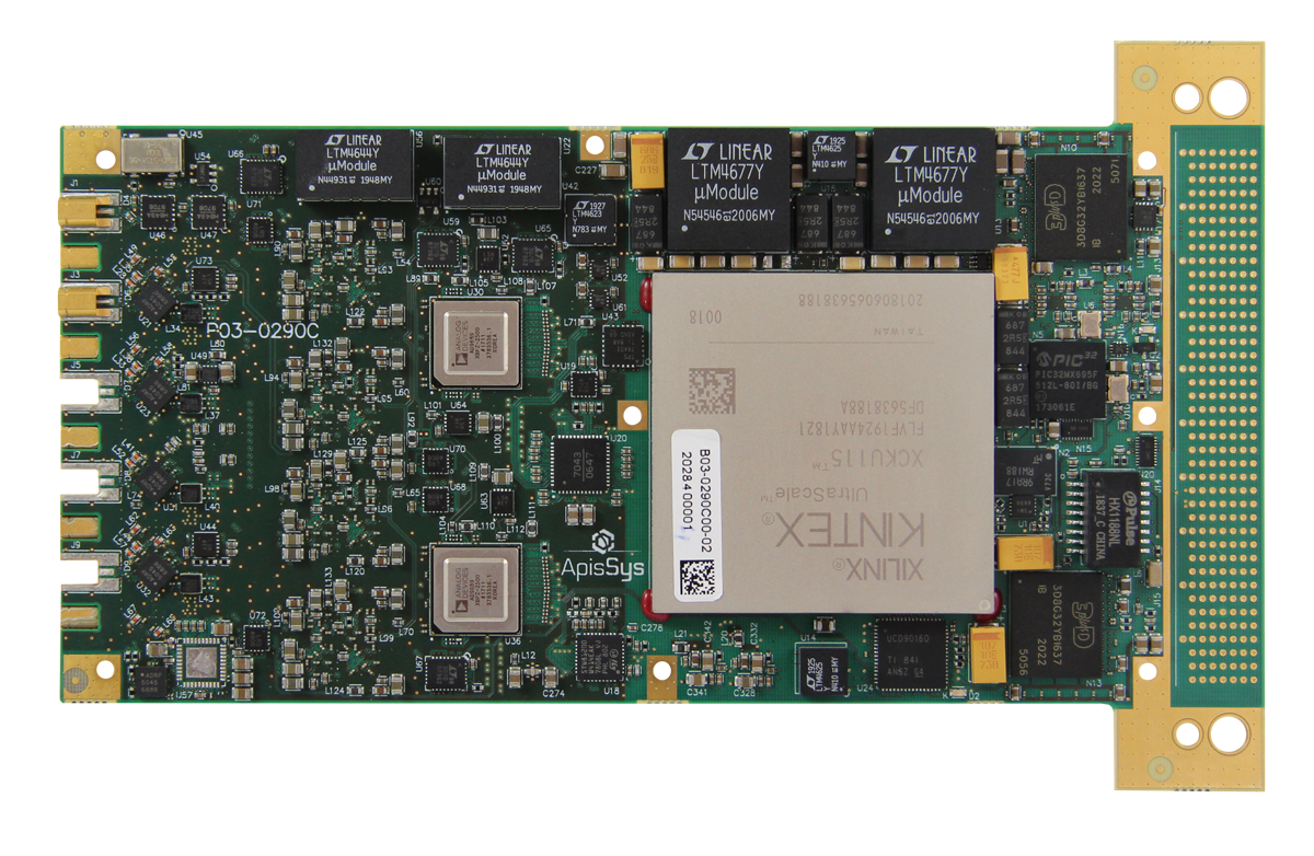
Presentation of the AV150 VPX board, for high resolution and general purpose applications
The AV150 is a component of apissys’ line of High-Speed data conversion and signal processing solutions, which adhere to the VITA 47, VPX standard.
Fully compliant with the OpenVPX standard, the AV150 supports a variety of communication protocols, including PCIe, Gigabit Ethernet and Aurora, as well as a large number of user-defined I/O.
The AV150 combines four 14-bit 3 Gsps ADCs and four 16-bit 6/12 Gsps DAC with ultra-high processing power delivered by an AMD Virtex® Ultrascale+™ FPGA (VU7P/VU9P/VU13P).
AMD Virtex® UltraScale+™ FPGAs provide the highest performance and integration capabilities in a 14 nm/16 nm FinFET node. In addition, they offer the highest transceiver bandwidth, highest DSP count, and highest on-chip and in-package memory available in the UltraScale™ architecture. Virtex® UltraScale+™ FPGAs also provide numerous power options that deliver the optimum balance between the required system performance and the smallest power envelope.
Target markets of this AV150 VPX board include Phased-Array Radar Transmitter / Receiver, Electronic Warfare ESM /ECM, MIMO and Wideband Communication.
Featuring an internal ultra-low jitter reference and a clock synthesizer, the AV150 offers versatility by allowing the use of either external clock or external reference for increased flexibility.
The AV150 includes one AMD Virtex® Ultrascale+™ FPGA (VU7P/VU9P/VU13P). Within a 14 nm/16 nm FinFET node, AMD Virtex® UltraScale+™ FPGAs stand out for their exceptional performance and integration capabilities. They boast the highest transceiver bandwidth, DSP count, and on-chip/in-package memory within the UltraScale™ architecture. Moreover, Virtex® UltraScale+™ FPGAs offer a range of power options, allowing for an optimal balance between system performance requirements and power consumption constraints.
Equipped with a USB 2.0 interface designed for system monitoring and supervision, the AV150 offers comprehensive software drivers for both Windows and Linux platforms. Additionally, it includes an FPGA Development Kit containing all essential cores required to construct user FPGA applications.
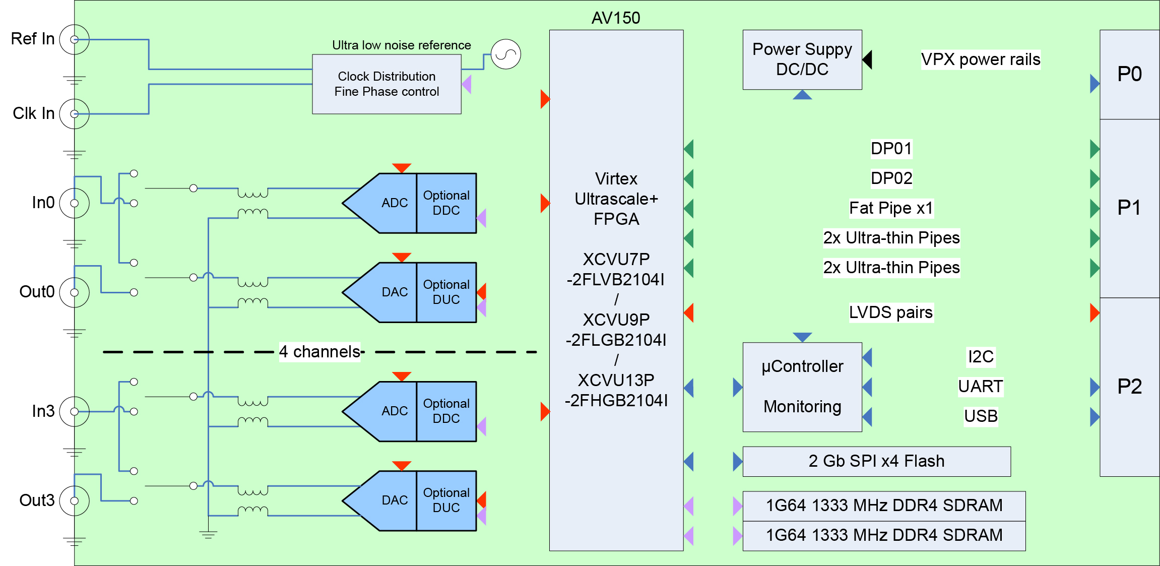
Analog Inputs/Outputs
Analog-Digital Conversion
Digital-Analog Conversion
Clock
Digital Down Converter
Digital Up Converter
FPGA
Memory
Software support
Firmware support
Operating Temperature
Power dissipation (VU13P)
Weight
VPX interface
| Part Number | AV150 | c | a | b | |
|---|---|---|---|---|---|
| Cooling | Air Conduction |
- - |
A C |
- - |
- - |
| FPGA | FPGA Virtex Ultrascale+ VU7P FPGA Virtex Ultrascale+ VU9P FPGA Virtex Ultrascale+ VU13P |
- - - |
- - - |
7 9 13 |
- - - |
Availability: September 2024
| Environmental | Air-cooled Vita 47 class EAC4 | Conduction-cooled Vita 47 class ECC3 |
| Operating Temperature |
0°C to 55C (8 CFM airflow at sea level) |
-40°C to +70°C (Card Edge) |
| Non Operating Temperature |
-40°C to +85°C | -50°C to +100°C |
| Operating Vibration (Random) |
5Hz - 100Hz +3 dB/octave 100Hz - 1kHz = 0.04 g2/Hz 1kHz - 2kHz -6 dB/octave |
5Hz - 100Hz +3 dB/octave 100Hz - 1kHz = 0.01g2/Hz 1kHz - 2kHz -6 dB/octave |
| Operating Shock | 20g, 11 millisecond, half-sine |
40g, 11 millisecond, half-sine |
| Operating Relative Humidity | 0% to 95% non-condensing | 0% to 95% non-condensing |
| Operating Attitude | 0 to 10’000 ft with adequate airflow |
-1,500 to 60,000 ft |
The AV129 is part of apissys’ range of High Speed data conversion and signal processing solutions based on the VITA 46, VPX standard.
The AV129 is fully compliant with OpenVPX standard, accommodating various communication protocols such as PCIe, SRIO, 1 Gbit and XAUI 10 Gbit Ethernet, as well as non OpenVPX adopted standard such as Aurora.
The AV129 combines four 14-bit 3 Gsps ADCs and four 16-bit 6/12 Gsps DAC with ultra-high processing power delivered by Xilinx® Kintex® Ultrascale™ FPGA, making it ideally suited for fully synchronous multiple channels test and measurement, MIMO, Electronic Warfare or Ultra-Wideband Radar Transceiver applications.
The AV129 features an internal ultra-low jitter reference and one clock synthesizer and can be used with either external clock or external reference for higher flexibility.
The AV129 includes one Xilinx® Kintex® Ultrascale™ KU115 FPGA for an impressive processing capability of more than 7 TMACs (Multiply Accumulate per second), two high speed 256M64 DDR3 SDRAM memory for data processing and two 1 Gb synchronous FLASH memory for multiple firmware storage.
The AV129 provides a USB 2.0 interface and a 10/100 Ethernet interface intended to be used for system monitoring and supervision.
The AV129 comes with complete software drivers for Windows and Linux. An FPGA Development Kit is provided including all necessary cores to build user FPGA application.